(Phys.org) –As silicon-based electronics are predicted to reach their absolute limits on performance around 2020, new technologies have been proposed to continue the trend in the miniaturization of electronic devices. One of these approaches consists of constructing field-effect transistors (FETs) directly on carbon nanotubes (CNTs). The resulting devices are on the scale of mere nanometers, although their fabrication is still a challenge.
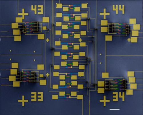
Now in a new paper published in Nano Letters, researchers Tian Pei, et al., at Peking University in Beijing, China, have developed a modular method for constructing complicated integrated circuits (ICs) made from many FETs on individual CNTs. To demonstrate, they constructed an 8-bits BUS system–a circuit that is widely used for transferring data in computers–that contains 46 FETs on six CNTs. This is the most complicated CNT IC fabricated to date, and the fabrication process is expected to lead to even more complex circuits.

SEM image of an eight-transistor (8-T) unit that was fabricated on two CNTs (marked with two white dotted lines). The scale bar is 100 μm. (Copyright: 2014 American Chemical Society)
Ever since the first CNT FET was fabricated in 1998, researchers have been working to improve CNT-based electronics. As the scientists explain in their paper, semiconducting CNTs are promising candidates for replacing silicon wires because they are thinner, which offers better scaling-down potential, and also because they have a higher carrier mobility, resulting in higher operating speeds.
Yet CNT-based electronics still face challenges. One of the most significant challenges is obtaining arrays of semiconducting CNTs while removing the less-suitable metallic CNTs. Although scientists have devised a variety of ways to separate semiconducting and metallic CNTs, these methods almost always result in damaged semiconducting CNTs with degraded performance.
To get around this problem, researchers usually build ICs on single CNTs, which can be individually selected based on their condition. It's difficult to use more than one CNT because no two are alike: they each have slightly different diameters and properties that affect performance. However, using just one CNT limits the complexity of these devices to simple logic and arithmetical gates.

SEM image of a BUS circuit based on five semiconducting CNTs selected through electrical measurements. The scale bar is 50 μm. (Copyright: 2014 American Chemical Society)
In the new study, the researchers from Peking University demonstrated that it's possible to efficiently build complex ICs on multiple CNTs, even though the CNTs have different properties. They did this using a modular approach, with the basic module being an eight-transistor (8-T) unit built on two CNTs with different electronic properties. The 8-T unit shows excellent tolerance to the property difference between the CNTs and can be used as a building block to fabricate the 8-bits BUS system, which contains 46 FETs on six CNTs. Tests showed that the 8-bits BUS system maintains a strong signal even as it passes through seven cascading logic gates.
As the researchers explain, the method is particularly valuable now because it allows for exploration of the performance limits of CNT ICs while the material problems are still being solved.
"This work has laid down a general way to construct complicated integrated circuits using currently non-perfect carbon nanotube materials, which (unlike silicon) are one-dimensional and different from each other," Lian-Mao Peng, Professor at Peking University and coauthor of the new paper, told Phys.org.
The 8-T unit can be used as the basic building block of a variety of ICs other than BUS systems, making this modular method a universal and efficient way to construct large-scale CNT ICs. Building on their previous research, the scientists hope to explore these possibilities in the future.
"In our earlier work, we showed that a carbon nanotube based field-effect transistor is about five (n-type FET) to ten (p-type FET) times faster than its silicon counterparts, but uses much less energy, about a few percent of that of similar sized silicon transistors," Peng said.
"In the future, we plan to construct large-scale integrated circuits that outperform silicon-based systems. These circuits are faster, smaller, and consume much less power. They can also work at extremely low temperatures (e.g., in space) and moderately high temperatures (potentially no cooling system required), on flexible and transparent substrates, and potentially be bio-compatible."
More information: Tian Pei, et al. "Modularized Construction of General Integrated Circuits on Individual Carbon Nanotubes." Nano Letters. DOI: 10.1021/nl5001604
Reported by: Lisa Zyga
Source: Phy.org
Edited by: Arthars