Discovery of zero-energy bound states at both ends of a one-dimensional atomic line defect
Mar 13, 2020
Peking University, March 13, 2020: In recent years, the development of quantum computers beyond the capability of classical computers has become a new frontier in science and technology and a key direction to realize quantum supremacy. However, conventional quantum computing has a serious challenge due to quantum decoherence effect and requires a significant amount of error correction in scaling quantum qubits. Therefore, the exploration of fault-tolerant quantum computation using quantum states topologically protected against local environmental perturbations is an important endeavor of both fundamental value and technological significance for realizing large-scale quantum computation.
Majorana zero-energy bound states (ZEBSs) in condensed matter systems such as superconductors are such rare quantum states with topological protection against local perturbations. These so called Majorana zero modes (MZMs) are charge neutral and obey non-abelian exchange statistics and serve as the building block of topological qubits. MZMs are theoretically predicted to exist in the vortex core of p-wave topological superconductors or at the ends of one-dimensional (1D) topological superconductors. Being a ZEBS, one of the main characteristics of the MZM is the differential conductance peaks for tunneling at zero bias voltage. Experimentally, the current Majorana platforms include the following. One is using a three-dimensional (3D) topological insulator proximity-coupling to an s-wave superconductor to realize the superconducting topological surface states and detect the vortex states by applying a magnetic field. The other one is using a 1D spin–orbit coupling nanowire proximity-coupling to an s-wave superconductor to detect zero-bias conductance peaks at the ends under an external magnetic field. However, the complicated fabrication of the hybrid structures, the extremely low temperature and the applied magnetic field required for observation present great challenges to the possible application of MZMs.
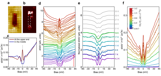
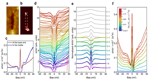
Recently, Professor Wang Jian’s group at Peking University, in collaboration with Professor Wang Ziqiang’s group at Boston College, discovered MZMs at both ends of 1D atomic line defects in two-dimensional (2D) iron-based high-temperature superconductors and provided a promising platform to detect topological zero-energy excitations at a higher operating temperature and under zero external magnetic field. Wang Jian’s group successfully grew large-area and high-quality one-unit-cell-thick FeTe0.5Se0.5 films on SrTiO3(001) substrates by molecular beam epitaxy (MBE) technique, which show Tc (~62 K) much higher than that (~14.5 K) in bulk Fe(Te,Se). By in situ low-temperature (4.2 K) scanning tunneling microscopy/spectroscopy (STM/STS), the 1D atomic line defects formed by the missing topmost Te/Se atoms can be clearly identified on the monolayer FeTe0.5Se0.5 films. The ZEBSs are detected at both ends of the 1D atomic line defect (Figure 1), while the tunneling spectra in the middle of the line defect recover to the fully gapped superconducting states. As the temperature increases, the ZEBS reduces in intensity, and finally vanishes at a temperature (around 20 K) far below Tc. The ZEBS does not split with increasing tunneling barrier conductance and becomes sharper and higher as the tip approaches the film, showing the robust property. Moreover, on the shorter defect chain, the coupling between the ZEBSs at both ends leads to reduced zero-bias conductance peaks even in the middle section of the atomic line defect chain (Figure 2). The positive correlation between the zero-bias conductance and line defect lengths can be deduced from the statistics. The spectroscopic properties of the ZEBSs, including the evolution of the peak height and width with temperature, the disappearing temperature of ZEBS, the tunneling spectra in tip-approaching-sample process, as well as unsplit property are found to be consistent with the MZMs interpretation. Other possibilities such as Kondo effect, conventional impurity states or the Andreev zero-energy bound states in nodal high-temperature superconductors can be excluded in general.
Professor Wang Ziqiang’s group at Boston College proposed a possible theoretical explanation by extending the band theory of the Shockley surface state to the case of superconductors. Due to the large spin-orbit coupling, the 1D atomic line defect in monolayer FeTe0.5Se0.5 film may become an emergent 1D topological superconductor and a Kramers pair of MZMs appearing at the ends of the line defect protected by time-reversal symmetry. Even without time-reversal symmetry along the line defect, the 1D topological superconductor can also be realized with a single MZM located at each end of the chain. This work, for the first time, reveals a class of topological zero-energy excitations at both ends of 1D atomic line defects in 2D high-temperature superconducting monolayer FeTe0.5Se0.5 films, which show the advantages of being a single material, higher operating temperature and zero external magnetic field, and may offer a new platform for future realizations of applicable topological qubits.
The paper was published online by Nature Physics on March 9, 2020 (DOI: 10.1038/s41567-020-0813-0). Links to the paper: https://www.nature.com/articles/s41567-020-0813-0. Professor Wang Jian at Peking University is the corresponding author and Chen Cheng at Peking University is the first author of this paper. Professor Wang Ziqiang’s group at Boston College are theoretical collaborators. This work is supported by the National Natural Science Foundation of China, the National Key Research and Development Program of China, Collaborative Innovation Center of Quantum Matter, the Strategic Priority Research Program of Chinese Academy of Sciences, Beijing Natural Science Foundation, and the US Department of Energy, Basic Energy Sciences.
Figure 1. ZEBSs at the ends of a long atomic line defect (about 15 Te/Se atoms in length). a, An STM topographic image of the long 1D atomic line defect. b, Spatial zero-energy mapping. c, Tunnelling spectra measured at the lower end and in the middle of the atomic line defect. d, Tunnelling spectra taken along the red arrow direction in a. e, The temperature evolution of the ZEBS at the bottom end of the line defect. The coloured curves are normalized tunnelling spectra and the grey curves are the 4.2-K spectra convoluted by the Fermi–Dirac distribution function at higher temperatures. f, The tunnelling barrier dependence of the ZEBS at the bottom end of the line defect.

Figure 2. ZEBSs at the ends of a short atomic line defect (about 8 Te/Se atoms in length). a, An STM topographic image of the short 1D atomic line defect. b, Spatial zero-energy mapping. c, Tunnelling spectra measured at the upper end and in the middle of the atomic line defect. d, Tunnelling spectra taken along the red arrow direction in a. e, The temperature evolution of the ZEBS at the top end of the line defect. The coloured curves are normalized tunnelling spectra and the grey curves are the 4.2-K spectra convoluted by the Fermi–Dirac distribution function at higher temperatures. f, The tunnelling barrier dependence of the ZEBS at the top end of the line defect.
Edited by: Huang Weijian
Source: School of Physics, Peking University

